Layer-by-Layer Phase Changes
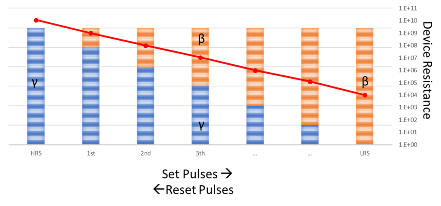
PCM devices offer strong scalability and low power consumption for the future of memory storage and computing. However, multistate operation is a key requirement for high density storage or operation in neuromorphic systems. Previous studies on In2Se3 based memory devices report a simple, two state (HRS, LRS) electrical configurationwhich has also been observed in other 2D materials. On the other hand, prelimnary transport measurensts with a 4-probe STM system reveleaed a much more interesting, multi-state switching behavior which covers six orders of magnitude range in device resistance.

These results from localized transport measurements conducted with a multi-probe STM system on gold/graphene/In2Se3 vertical phase change memory devices show resistance changes exponentially with the number of switching steps. This indicates the existence of a novel, layer by layer phase change within the In2Se3 film. I'm working to investigate this resistive switching behavior with more multi-probe STM measurements paired with cross-section TEM. Determining the role of interfaces whether it be the vdW gaps between the phases within In2Se3 and between In2Se3 and graphene or gold, can have great relevance to solid state devices