Memristor effect in 2D materials
STM is a powerful characterization techinque providing imaging at atomic resolution as well as equally precise probing tool. STM is limited to reasonably flat and conducting samples, but fortunately this makes it an ideal tool to study most 2D materials.
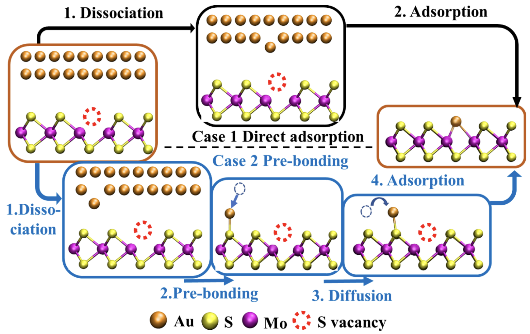
My colleagues were the first to report the observation of stable, non-volatile resistive switching with monolayer insulating or semiconducting 2D materials in vertical metal-insulator-metal device configurations. Furthermore, we revealed a one-to-one correlation between gold atom substituion into sulfur vacanices and the nonvolatile change in ressitance of MoS2 monolayers with STM for imaging, spectroscopy, and transport measurements. This led the development of the dissociation-diffusion-adsorbption (DDA) model to study the kinetics of resistive switching.

My work looks to expand upon the Au-MoS2 model system with an atomic-level investigation of Ag-hBN devices. I look to answer two fundamental questions:
- What is the role of defects in hBN in resistive switching?
- What is the role of imperfections in Ag surface layers in the DDA model?
Ge, R., Wu, X., Liang, L., Hus, S. M., Gu, Y., Okogbue, E., Chou, H., Shi, J., Zhang, Y., Banerjee, S. K., Jung, Y., Lee, J. C., & Akinwande, D. (2020). A Library of Atomically Thin 2D Materials Featuring the Conductive-Point Resistive Switching Phenomenon. In Advanced Materials (Vol. 33, Issue 7). Wiley. https://doi.org/10.1002/adma.202007792